What are Thin Film Solar Panels?

The details about thin film solar panels.
In recent years we have seen radical improvements in the underlying technology of solar panels and although you are familiar with the traditional-style solar panels in pictures and on rooftops, thin film solar panels are now making their way into the mainstream. They are called ‘thin film’ because they are able to be produced in such a way that allows them to be flexible and coat materials other than the standard wafer boards. This allows for many more applications for solar power and can allow them to blend more seamlessly into your home’s aesthetics.
The Difference Between Traditional Solar Panels and Thin Film
The most obvious difference between the traditional silicon wafer solar panel and newer thin film varieties is the thickness. There are also currently gaps in solar capture efficiencies between first-generation silicon-based wafers and newer, second-generation methods that use different compounds. This comes down to the materials being used in the panels themselves.
Traditional panels often use crystalline silicon (c-Si) in their manufacture. This process has been around for years and has established itself to be reliable. It should be mentioned that although c-Si is considered to have a high-efficiency rate in terms of energy production from installed systems, it is actually a relatively poor absorber of light. This means that the cells must be fairly thick and rigid in order to produce effectively.
Related: Comparing Solar Panel Types
In contrast, thin film technologies employ different elements that allow the cells to be up to 350 times thinner than the traditional wafer. This material can then be layered over coated glass, metal, or plastic to create a solar cell, and allows for many different types of materials and objects to produce energy.
Main Types of Thin Film Solar Cells
There are two main goals for thin film solar cells today: to have the flexibility to attach it to a larger variety of building materials and to eventually achieve the same or higher efficiency than traditional silicon-based methods. All of these methods below offer some differences in pros and cons compared to the traditional-style panels. Their names usually derives from the type of material that is used for its semiconductor. Let’s take a look at four and see how the different technologies compare:
#1: Amorphous Silicon (a-Si)
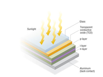
a-Si photovoltaic cell structure. Image by Alfred Hicks/NREL.gov
Amorphous Silicon is the oldest and most mature type of thin film to produce solar power. This is likely because silicon was already being used in its crystalline form to produce the more traditional panels and silicon’s electrical properties were well understood.
Pros:
- Unlike crystalline silicon, the amorphous silicon version actually has a very high solar absorption rate which makes very thin layers of the material possible. This effectively reduced material costs and because it is relatively abundant, nontoxic, and inexpensive it quickly became the first thin film method to break into the mainstream.
Cons:
- Because of its relatively low efficiency, however, you will mostly only see this method used in small-scale, flexible power packs and electronics.
#2: Cadmium Telluride (CdTe)
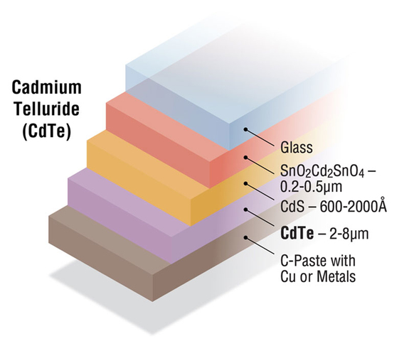
CdTe photovoltaic cell structure. Image by Alfred Hicks/NREL.gov
Solar technology based on cadmium telluride is now the second most popular PV technology in the world, sitting at around 5%. This is thanks to the fact that manufacturing of this process is cheaper and quicker than comparable silicon-based methods and recent leaps in efficiency have prompted more mainstream adoption.
Pros:
- As mentioned before, CdTe is cheaper than silicon-based methods, but it is important to note that by 2014 the technology had the smallest overall carbon footprint and payback time from purchase. Although CdTe, as well as thin film cells in general, lag behind the traditional c-Si panels in terms of efficiency, they have been rapidly approaching that gold standard. As of 2015, a company called First Solar reached an average commercial module efficiency of 16.1%.
- CdTe panels are also highly adaptable to hot, humid weather and low light when compared to traditional cells. This means that they work best in the areas with the most sun and are able to be used in areas that up until now were less than ideal.
Cons:
- One possible disadvantage of the CdTe method lies in the very materials used to manufacture them. Cadmium, by itself, is a very toxic substance that can accumulate in the food chain much like Mercury. Early results show that cadmium can leach from the compound over time in landfills and CdTe itself has shown toxic effects when inhaled by test rats. Fortunately, proper handling and disposal methods will negate much of the potential concern.
- As such, many agencies and laboratories are actively searching for alternatives that are safe for the environment while also being efficient. Current manufacturers are also searching for ways to reuse or recycle these materials as a way to help solve the issues concerning the environment.
#3: Copper Indium Gallium Diselenide (CIGS)
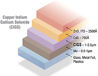
CIGS photovoltaic cell structure. Image by Alfred Hicks/NREL.gov
This type of solar cell is another popular type of semiconductor used to create thin film applications. The CIGS method is currently more popular in Europe and Japan, but there are manufacturers all over the world making use of this technique to take advantage of its environmentally safe materials and peak efficiency potential.
Pros:
- CIGS have the benefit of being environmentally friendly in terms of materials used which is a boon for manufacturers looking for a long-term benefit to the planet. The materials used also allow it to have the highest potential efficiency of any of the thin-film technologies as well as a great resistance to heat. There is also a great potential for long-life applications due to the lack of significant degradation over time.
- The methods used also allow for extremely thin sizes of less than one micrometer to be used in creating devices. This means that there are even more potential applications for this technology such as building materials, cars, and airplanes.
Cons:
- CIGS technology has yet to reach or surpass the traditional silicon-based panels, but it has made great leaps forward in recent years. Although the record for lab-based efficiency is over 20%, real-world applications still fall in the mid-teens.
#4: New Copper Zinc Tin Sulphur (CZTS) Method
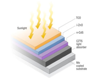
CZTS photovoltaic cell structure. Image by Alfred Hicks/NREL.gov
In an ongoing effort to find solar technology that is both environmentally friendly as well as manufactured using abundant materials, the CZTS method was discovered. This method is very similar to CIGS in terms of properties and methods of fabrication, but its efficiency is still very low.
Pros:
- As mentioned before, CZTS is made up of the earth-abundant elements copper, zinc, tin, and sulfoselenide. This means that the compound is both environmentally friendly and could ultimately become quite cheap because of the material cost. The tellurium and indium found in the CdTe and CIGS models are extremely rare, for instance.
Cons:
- CZTS is still in the early stages of development and in order to be more commercially viable, higher efficiencies are required. The technology current taps out at around 7.6%. It would need to hit around 20% efficiency before it could become competitive among its peers.
Conclusion
We trust this information has helped shed light on what exactly are thin film solar panels and how they are shaping the current landscape of solar energy production.
As these technologies mature, they will make their way into competitive products available for purchase. Already there are alternative methods of solar production, such as solar roof tiles, that allow customers to have a more aesthetically pleasing look while still saving money on their energy bills. Watch this space to see what innovative and new trends will be developed.
Photos courtesy of NREL.gov